

Photovoltaic Cells
The INPHAZE Impedance Spectrometer is able to measure the phase angle at each frequency with unprecedented precision and enables it to:
- Resolve nano-scale and atomic scale detail in well defined structures
- Resolve the depletion layers in photovoltaic cells
- Characterise charge carrier transport processes, resolve and charaterise the p (or n) regions in thin film cells, and charge injection capacitances etc.
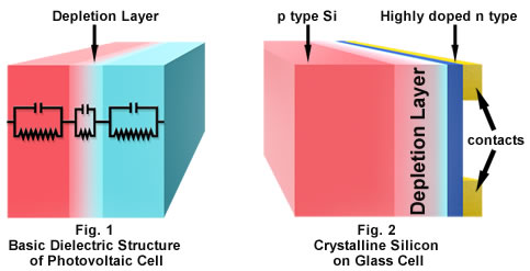
Semiconductor photovoltaic cells contain several distinct regions; the p region, n region and depletion layer at the junction of these semiconductor regions (Fig.1).
The depletion layer is generally several hundred nanometers in thickness whilst the dimensions of the p and n regions depend on the type of cell. For thin film cells the thickness of these regions may be similar to or thinner than that of the depletion layer.
The thin crystalline silicon on glass solar cells is one such example (Fig 2).
Because of the heavy doping of the n layer the depletion layer in these devices extends almost entirely into the p region.
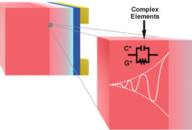
Charge Injection and Diffusion Polarisation Effects
Alternating buildup and depletion of carriers at the depletion layer boundary when an AC current is passed through the system is counterbalanced by electron-hole re-combination and back diffusion. This creates a decaying, propagated charge wave as depicted schematically.
Such a polarisation effect leads to an impedance element with complex capacitances and conductances. The dispersion due to the polarisation layer is discernable only at very low frequencies. At high frequencies there is insufficient time for the carrier concentrations to build up in each half cycle of the AC current.
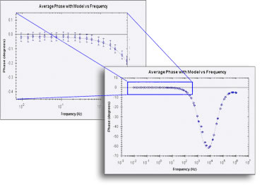
Experimental Data - Measurments of the conductance, capacitance and phase of a thin film solar cell.
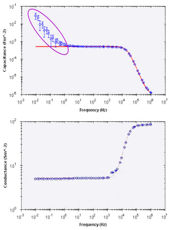
- At frequencies >1 Hz the results can be accurately fitted to a 2-layer model (p layer and depletion layer)
- At frequencies <1 Hz the capacitance increases dramatically with decreasing frequency (shown encircled). This is due to the diffusion polarisation impedance elements. While the phase angle in this regime is very small, the capacitance, as a function of frequency can still be determined (see diagram) by the INPHAZE spectrometer because of its very high phase resolution of 0.001 degrees, and this allows characterization of the diffusion polarisation effects.
- These measurements allow the dielectric structure of the depletion layer and the p region outside it to be determined as well as the characterisation of the charge injection and diffusion processes.
| download the PDF application note |  |
|
